diff options
| author | UnavailableDev <ggwildplay@gmail.com> | 2023-02-15 20:29:30 +0100 |
|---|---|---|
| committer | UnavailableDev <ggwildplay@gmail.com> | 2023-02-15 20:29:30 +0100 |
| commit | b1502e3a2f542b509dcfcf73b31b0613306a9c1e (patch) | |
| tree | c4308e151f1bc8eb5025de062f81bb4f060f7473 | |
| parent | 1e7848653e1f0ee2fd578491dbc215dcdce6f08b (diff) | |
Quick spelling check
| -rw-r--r-- | docs/architecture.md | 10 | ||||
| -rw-r--r-- | docs/research.md | 20 |
2 files changed, 15 insertions, 15 deletions
diff --git a/docs/architecture.md b/docs/architecture.md index 055d228..191a635 100644 --- a/docs/architecture.md +++ b/docs/architecture.md @@ -30,14 +30,14 @@ For this reason the input will be handled by the microcontroller as this will im The controller will have four buttons, so 4 data pins are needed on the microcontroller plus a ground and 3.3V or 5V pin. In total there are 6 pins needed. If the game is going to be played by 2 person, there are 4 more data pins needed so 8 data pins for both controllers. -For data transfer between STM32 and FPHA there are 4 pins needed at maximum (SPI for instance). +For data transfer between STM32 and FPGA there are 4 pins needed at maximum (SPI for instance). The STM32 will be used and most STM32 boards have enough I/O pins for our needs. -The STM32 F030 and F091 provided by AVANS both have 15 digital pins and 6 analog pins. +The STM32 F030 and F091 provided by Avans both have 15 digital pins and 6 analog pins. The buttons will be connected as follows: 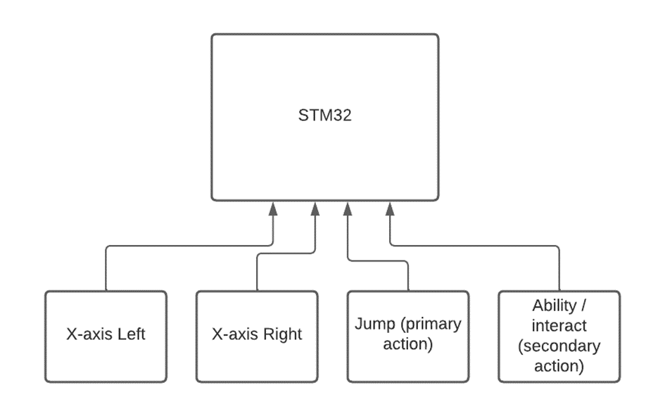 -To implement the input in the game, the input should be ckecked at the start of each game cycle. In this case there are no interupts needed. +To implement the input in the game, the input should be checked at the start of each game cycle. In this case there are no interrupts needed. # STM32 software @@ -87,9 +87,9 @@ Notable differences: - 8 total palettes, with 8 colors each More colors is better. Increasing the total palette count is a very memory - intensive operation, while increaing the palette color count is likely slower + intensive operation, while increasing the palette color count is likely slower when looking up color values for each pixel on real hardware. -- Sprites can be positioned paritally off-screen on all screen edges using only +- Sprites can be positioned partially off-screen on all screen edges using only the offset bits in the FAM register The NES has a separate PPUMASK register to control special color effects, and diff --git a/docs/research.md b/docs/research.md index 682ed43..d153143 100644 --- a/docs/research.md +++ b/docs/research.md @@ -101,7 +101,7 @@ int main() { ``` # Generating audio signals -In order to generate sound for this project, a few posibilities exist (see chapters below) +In order to generate sound for this project, a few possibilities exist (see chapters below) ## Sound chips @@ -120,9 +120,9 @@ A sound chip is made to use digital, analog or mixed signals and produce a tone | Texas Instruments | [SN76489](https://en.wikipedia.org/wiki/SN76489 "SN76489") | 1980 | 4 | Yes | N/A | | Texas Instruments | [Sega PSG (SN76496)](https://en.wikipedia.org/wiki/SN76496 "SN76496") | 1982 | 4 | Yes | N/A | -This chart shows different audio chips that might have been used in retro consoles. While all of them aren't easily available anymore it is still interesting to take a close look at how these IC's (Intergrated Ciruit) work. +This chart shows different audio chips that might have been used in retro consoles. While all of them aren't easily available anymore it is still interesting to take a close look at how these IC's (Integrated Circuit) work. -Most chips work on one of two pricibles, this being either a "Programmable sound generator" or "Sound Chip" +Most chips work on one of two crucibles, this being either a "Programmable sound generator" or "Sound Chip" ### Programmable sound generator (PSG) @@ -139,9 +139,9 @@ In order to create an audio signal using the FPGA we can use PWM to emulate an a  -This figure shows an example signal (in blue), created by the FPGA. and the corosponding analog signal (in red). +This figure shows an example signal (in blue), created by the FPGA. and the corresponding analog signal (in red). -It is usefull to generate a few different types of signals like: +It is useful to generate a few different types of signals like: - triangle waves - square waves - sine waves @@ -154,7 +154,7 @@ There are a lot of ways to make a 2d level but because where using an microcontr ## pictures if a level is made there is a possibility that it can be exported as a picture. You can use that picture format and decode it in the microcontroller then send it to the FPGA that sends that data through the VGA. the problem with this method is that a lot of data is needed to save a whole level (640 * 480 pixels) but different formats can have a large impact. For a better reference picture below. - + ### PNG PNG (Portable Network Graphics) is a lossless image compression format. Resulting in high-quality images that preserve all of the original data. Additionally, PNG supports a wider range of color depths, including 24-bit RGB and 32-bit RGBA (which includes an alpha channel for transparency), making it well-suited for images with a large number of colors or images that require transparency. @@ -181,7 +181,7 @@ indexes is another way of using tiles and colors at a 2d level. With this method in the picture, you can have a better understanding of how indexes work. ### Data the color palette is saved on the FPGA with the different tiles. While the microcontroller makes the levels and sends the indexed tiles to the FPGA. - + ### conclusion This method of creating levels splits the memory between the FPGA and the microcontroller. Additionally, the complexity behind the program is smaller while still giving a lot of freedom with level creation. @@ -230,11 +230,11 @@ The FPGA code contains multiple entities. Data transfer between these entities takes at least one clock cycle. If there are multiple entities the delay will increase and decreases the playability of the game. -## Conlcusion +## Conclusion For gameplay reasons it is recommended to have the input handling as close as possible to the game logic unit. This will decrease the delay between the user-input and onscreen gameplay. -# Microcontroller FGPA communication +# Microcontroller FPGA communication The hardware of the game consist out of a microcontroller(stm32) and a FPGA(basys3). The hardware components needs to communicate with each other. For this a protocol is needed. See table 1 for a comparison of possible protocols: @@ -248,5 +248,5 @@ See table 1 for a comparison of possible protocols: There are only two devices that has to be connected. Complexity and master/slave amount are not relevant for this purpose. If there are multiple entities the delay will increase and decreases the playability of the game. -## Conlcusion +## Conclusion It is recommended that SPI will be the communication protocol because of the data transfer speeds. The is a lot of data transfer between the microcontroller and FPGA. |