1
2
3
4
5
6
7
8
9
10
11
12
13
14
15
16
17
18
19
20
21
22
23
24
25
26
27
28
29
30
31
32
33
34
35
36
37
38
39
40
41
42
43
44
45
46
47
48
49
50
51
52
53
54
55
56
57
58
59
60
61
62
63
64
65
66
67
68
69
70
71
72
73
74
75
76
77
78
79
80
81
82
83
84
85
86
87
88
89
90
91
92
93
94
95
96
97
98
99
100
101
102
103
104
105
106
107
108
109
110
111
112
113
114
115
116
117
118
119
120
121
122
123
124
125
126
127
128
129
130
131
132
133
134
135
136
137
138
139
140
141
142
143
144
145
146
147
148
149
150
151
152
153
154
155
156
157
158
159
160
161
162
163
164
165
166
167
168
169
170
171
172
173
174
175
176
177
178
179
180
181
182
183
184
185
186
187
188
189
190
191
192
193
194
195
196
197
198
199
200
201
202
203
204
205
206
207
208
209
210
211
212
213
214
215
216
217
218
219
220
221
222
223
224
225
226
227
228
229
230
231
232
233
234
235
236
237
238
239
240
241
242
243
244
245
246
247
248
249
250
251
252
253
254
255
256
257
258
259
260
261
262
263
264
265
266
267
268
269
270
271
272
273
274
275
276
277
278
279
280
281
282
283
284
285
286
287
288
289
290
291
292
293
294
295
296
297
298
299
300
301
302
303
304
305
306
307
308
309
310
311
312
313
314
315
316
317
318
319
320
321
322
323
324
325
326
327
328
329
330
331
332
333
334
335
336
337
338
339
340
341
342
343
344
345
346
347
348
349
350
351
352
353
354
355
356
357
358
359
360
361
362
363
364
365
366
367
368
369
370
371
372
373
374
375
376
377
378
379
380
381
382
383
384
385
386
387
388
389
390
391
392
393
394
395
396
397
398
399
400
401
402
403
404
405
406
407
408
409
410
411
412
413
414
415
416
417
418
419
420
421
422
423
424
425
426
427
428
429
430
431
432
433
434
435
436
437
438
439
440
441
442
443
444
445
446
447
448
449
450
451
452
453
454
455
456
457
458
459
460
461
462
463
464
465
466
467
468
469
470
471
472
473
474
475
476
477
478
479
480
481
482
483
484
485
486
487
488
489
490
491
492
493
494
495
|
<!-- # Hooded Havic: Miniboss Mania -->

# Introduction
Welcome to Hooded Havoc: Miniboss Mania, an exciting 2D platformer game created by our team Joshua, Loek, Bjorn, Frenk and Niels! This game was developed using the STM32 microcontroller as the game engine and the FPGA as the Picture Processing Unit (PPU).
In Hooded Havoc: Miniboss Mania, you will take on the role of a brave hero who must battle through multiple levels filled with challenging obstacles and formidable minibosses. With smooth gameplay and engaging graphics, you will feel immersed in a world of adventure and excitement.
Our use of the STM32 microcontroller and FPGA PPU allowed us to create a unique and innovative gaming experience. The STM32 provides efficient and reliable processing power, while the FPGA ensures that our graphics are rendered smoothly and accurately.
So get ready to embark on a thrilling journey through Hooded Havoc: Miniboss Mania, and see how far you can make it!
## Objective
The objective of Hooded Havoc: Miniboss Mania is to guide the hero through multiple levels, defeating minibosses and overcoming obstacles along the way. The ultimate goal is to reach the final boss and defeat them to retrieve the stolen staff.
To achieve this objective, the player must use their platforming skills to jump, run, and dodge obstacles while also battling enemies and minibosses. Each level presents a unique challenge that will require the player to adapt and strategize to overcome.
As the player progresses through the game, they will unlock new abilities and power-ups that will aid them in their journey. The player must use these abilities wisely to defeat the minibosses and ultimately save the world.
So, the objective of Hooded Havoc: Miniboss Mania is not only to provide an exciting and engaging gaming experience but also to challenge players to use their skills and strategic thinking to overcome obstacles and emerge victorious.
## Problem statement
One potential problem that could arise in the development of Hooded Havoc: Miniboss Mania is related to the PPU and communication between the STM32 and PPU.
The PPU is responsible for rendering the graphics and displaying them on the screen, while the STM32 is responsible for processing the game logic and input from the player. However, if there is a problem with the communication between these two components, it could lead to synchronization issues and graphical glitches that could affect the player's experience.
For example, if the PPU is unable to keep up with the processing speed of the STM32, the graphics may lag or appear distorted, causing the game to become unplayable. Similarly, if there is a delay in communication between the STM32 and PPU, it could result in a mismatch between the game logic and the displayed graphics, leading to confusion for the player.
To ensure a smooth and enjoyable gaming experience, it is essential to address any potential issues with the PPU and communication between the STM32 and PPU during the development process. This may involve optimizing the code for both components, adjusting the communication protocol, or adding buffer systems to prevent lag or synchronization issues.
# General system architecture
The existing hardware components available for building this project consists
of:
- Raspberry Pi
- Nucleo STM32 development board
- Basys3 FPGA development board
- Arduino Uno R3
The Raspberry Pi is by far the most powerful component out of these 4, but
because one of the project requirements is that no general-purpose operating
system is used, utilizing the Raspberry Pi will involve writing low-level
drivers for its interfaces, which will likely cost a lot of effort.
As to not risk project failure due to hardware constraints, the decision was
made to use the STM32 microcontroller and FPGA in combination, as these two are
both familiar and still relatively powerful platforms. Because audio and video
consist of data streams that require constant output, the audio and graphics
processing is outsourced to the FPGA. All other game logic processing such as
world loading, or map and entity interactions is done on the STM32
microcontroller.
Our game also supports an optional second player, as is shown in the following
diagram.

In the above diagram, the "display" and "speaker" components are included to
show what the complete system looks like. The scope of this project only
includes the components inside the area marked "game console" and the gamepad
components.
# STM32 software
The game engine is designed to run a 2D platformer game. The game engine has to manage all the different game states. To do this it will utilize a finite state machine (FSM). The game engine will also cover de input handling from the player, the game logic for example enemy handling or the powerup handling it will also send out data to the APU (Audio processing unit) so that the right sounds will be played.
FSM is a useful tool for managing game states and transitions. The game has many different states such as: title screen, shop and gameplay state. Each state represents a particular configuration from the with different logic and variables.
The state machine is designed to have the following states:
1. Initialization: The initialization state will be responsible for initializing all game-related variables and subsystems, including the FPGA-based picture processing unit.
2. Title Screen: The title screen state will display the game's title screen and wait for user input to start the game or access the options menu.
3. Options: The options state will allow the user to configure game settings, such as sound and graphics options.
4. Game Play: The game play state will be responsible for running the game logic and updating the game state.
5. Game Over: The game over state will display the game over screen and wait for user input to restart the game or return to the title screen.
## Input
The playable character has 4 actions that it can perform:
- horizontal movement
- aiming
- jump
- ability / use
To perform these action there will be 6 buttons for the user to use.
A joystick is not needed for the movement because the movement is not complex, so button fulfill this.
The layout will be as follows:
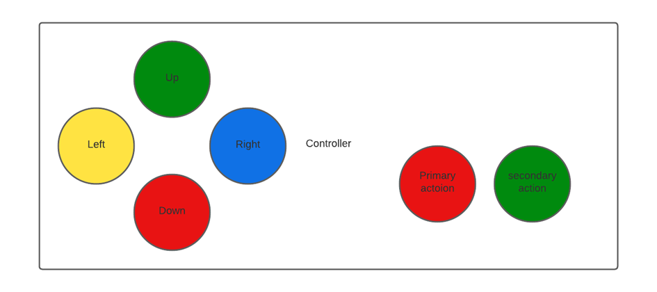
## Input handling
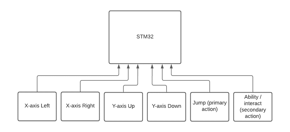
The hardware consist out of a microcontroller and a FPGA.
The microcontroller will process the game logic.
For this reason the input will be handled by the microcontroller as this will improve playability (stated in research).
The controller will have six buttons, so six data pins are needed on the microcontroller plus a ground and 3.3V or 5V pin.
In total there are eight pins needed.
If the game is going to be played by 2 persons, there are six more data pins needed so 8 data pins for both controllers.
For data transfer between STM32 and FPGA there are 4 pins needed at maximum (SPI for instance).
The STM32 will be used and most STM32 boards have enough I/O pins for our needs.
The STM32 F030 and F091 provided by Avans both have 15 digital pins and 6 analog pins.
The buttons will be connected as follows:
To implement the input in the game, the input should be checked at the start of each game cycle. In this case there are no interrupts needed.
## PPU communication
The SPI module will be configured that sends 8 bits per cycle and at a speed of 1.0 MB/s. The STM32 Cube IDE SPI module does not include a slave select line so a pin has to configured manually to fullfill this purpose. Every data transfer consists out of 4 times 8 bits, so 32 bits in total. The first byte is the address and the other 3 bytes consist the data.
## SPI
The FPGA uses 3 JMOD pins to receive the SPI data. The FPGA does not have a IP-Core for SPI. To receive the data the module has 3 synchronisers for the incoming SPI clock, data and slave select. The data will be read via the SPI protocol and shifted untill all 32 bits are read.
# PPU
As mentioned in the [research document](research.md#graphics), the PPU designed
for this project is heavily inspired by the NES's PPU. Because our game does
need slightly different graphical capabilities, the differences between the NES
PPU and our custom PPU are highlighted here. Readers of this section are
expected to know basic operation of the NES's PPU.
PPU features:
- 320x240 @ 60Hz VGA output (upscaled to 640x480)
- single tilemap with room for 1024 tiles of 16x16 pixels
- 8 colors per palette, with 4096 possible colors (12-bit color depth)
- 640x480 background canvas with scrolling
- NO background scrolling splits
- 128 total sprites on screen (NO scanline sprite limit)
- the first 16 foreground sprites have accurate background occlusion
- sprites are always drawn on top of the background layer
- PPU control using DMA (dual-port asynchronous RAM)
- tiles can be flipped using FAM or BAM
- no frame buffer
- vertical and horizontal sync and blank output
Notable differences:
- NES nametable equivalent is called BAM (background attribute register)
- NES OAM equivalent is called FAM (foreground attribute register)
- 320x240 @ 60Hz output
Since we're using VGA, we can't use custom resolutions without an
upscaler/downscaler. This resolution was chosen because it's exactly half of
the lowest standard VGA resolution 640x480. The native resolution can't be
used due to the pipelined pixel fetch logic, which needs at least 5 clock
cycles to produce a stable color output.
- No scanline sprite limit
Unless not imposing any sprite limit makes the hardware implementation
impossible, or much more difficult, this is a restriction that will likely
lead to frustrating debugging sessions, so will not be replicated in our
custom PPU.
- Sprites are 16x16
Most NES games already tile multiple 8x8 tiles together into "metatiles" to
create the illusion of larger sprites. This was likely done to save on memory
costs as RAM was expensive in the '80s, but since we're running on an FPGA
cost is irrelevant.
- Single 1024 sprite tilemap shared between foreground and background sprites
The NES OAM registers contain a bit to select which tilemap to use (of two),
which effectively expands each tile's index address by one bit. Instead of
creating the illusion of two separate memory areas for tiles, having one
large tilemap seems like a more sensible solution.
- 8 total palettes, with 8 colors each
More colors is better. Increasing the palette color count is a very memory
intensive operation, while increasing the total amount of palettes is slower
when looking up color values for each pixel on real hardware.
- Sprites can be positioned partially off-screen on all screen edges using only
the offset bits in the FAM register
The NES has a separate PPUMASK register to control special color effects, and
to shift sprites off the left and top screen edges, as the sprite offsets
count from 0. Our PPU's FAM sprite offset bits count from -16, so the sprite
can shift past the top and left screen edges, as well as the standard bottom
and right edges.
- No status line register, only vertical and horizontal blanking/sync outputs
are supplied back to CPU
The NES status line register contains some handy lines, such as a buggy
status line for reaching the max sprite count per scanline, and a status line
for detecting collisions between background and foreground sprites. Our PPU
doesn't have a scanline limit, and all hitbox detection is done in software.
Software hacks involving swapping tiles during a screen draw cycle can still
be achieved by counting the V-sync and H-sync pulses using interrupts.
- No background scrolling splits
This feature allows only part of the background canvas to be scrolled, while
another portion remains still. This was used to draw HUD elements on the
background layer for displaying things like health bars or score counters.
Since we are working with a higher foreground sprite limit, we'll use regular
foreground sprites to display HUD elements.
- Sprites are always drawn on top of the background layer
Our game doesn't need this capability for any visual effects. Leaving this
feature out will lead to a simpler hardware design
- Sprites are positioned relative to the viewport, not the background layer
This leads to a simpler hardware architecture for the foreground sprite
rendering component. Since the CPU is already likely to reposition all
foreground sprites on every frame, the position calculation is moved to
hardware to software.
## Hardware design schematics
### Top (level 1)

Important notes:
- The STM32 can reset the PPU. This line will also be connected to a physical
button on the FPGA.
- The STM32 uses direct memory access to control the PPU.
- The PPU's native resolution is 320x240. It works in this resolution as if it
is a valid VGA signal. The STM32 is also only aware of this resolution. This
resolution is referred to as "tiny" resolution. Because VGA-compatible LCD's
likely don't support this resolution due to low clock speed, a built-in
pixel-perfect 2X upscaler is chained after the PPU's "tiny" output. This
means that the display sees the resolution as 640x480, but the PPU and STM32
only work in 320x240.
- The STM32 receives the TVSYNC and THSYNC lines from the PPU. These are the
VSYNC and HSYNC lines from the tiny VGA signal generator. These lines can be
used to trigger interrupts for counting frames, and to make sure no
read/write conflicts occur for protected memory regions in the PPU.
- NVSYNC, NHSYNC and the RGB signals refer to the output of the native VGA
signal generator.
### Level 2

Important notes:
- The pixel fetch logic is pipelined in 5 stages:
1. - (Foreground sprite info) calculate if foreground sprite exists at
current pixel using FAM register
- (Background sprite info) get background sprite info from BAM register
2. - (Sprite render) calculate pixel to read from TMM based on sprite info
3. - (Compositor) get pixel with 'highest' priority (pick first foreground
sprite with non-transparent color at current pixel in order, fallback to
background)
- (Palette lookup) lookup palette color using palette register
- (VGA signal generator) output real color to VGA signal generator
- The pipeline stages with two clock cycles contain an address set and memory
read step.
- The pipeline takes 5 clock ticks in total. About 18 are available during each
pixel. For optimal display compatibility, the output color signal should be
stable before 50% of the pixel clock pulse width (9 clock ticks).
- Since the "sprite info" and "sprite render" steps are fundamentally different
for the foreground and background layer, these components will be combined
into one for each layer respectively. They are separated in the above diagram
for pipeline stage illustration.
- The AUX, FAM, and PAL registers are implemented in the component that
directly accesses them, but are exposed to the PPU RAM bus for writing.
- Each foreground sprite render component holds its own sprite data copy from
the RAM in it's own cache memory. The cache updates are fetched during the
VBLANK time between each frame.
<!-- inaccurate and no longer needed
### Level 3
This diagram has several flaws, but a significant amount of time has already
been spent on these, so they are highlighted here instead of being fixed.

Flaws:
- Pipeline stages 1-4 aren't properly connected in this diagram, see level 2
notes for proper functionality
- The global RESET input resets all PPU RAM, but isn't connected to all RAM
ports
- All DATA inputs on the same line as an ADDR output are connections to a
memory component. Not all of these are connected in the diagram, though they
should be.
- All ADDR and ADDR drivers are also tri-state. EN inputs need to be added to
support switching the output on/off.
Important notes:
- The background sprite and foreground sprite component internally share some
components for coordinate transformations
- The foreground sprite component is only shown once here, but is cloned for
each foreground sprite the PPU allows.
- The CIDX lines between the sprite and compositor components is shared by all
sprite components, and is such tri-state. A single sprite component outputs a
CIDX signal based on the EN signal from the compositor.
- All DATA and ADDR lines are shared between all RAM ports. WEN inputs are
controlled by the address decoder.
-->
## Pipeline stage reference

This diagram describes which components use which lines during pipeline stages
0-9. The pipeline stage counter is reset after every pixel, and is run on the
system clock (100 MHz). Underlined labels indicate when a signal is written,
and normal text is used to indicate a signal read. Labels with a dotted outline
are used for timing, but don't directly read/write any signals.
## Registers
- The PPU's memory bus has 16-bit addresses and 16-bit words.
- Some memory regions use physical word sizes smaller than 16-bits, so
"unneeded" bits will be discarded by the PPU.
- Apparent size means the amount of addresses in a given memory region. As
mentioned earlier, the exact word sizes of a memory area can vary, though
this is not visible to the CPU as all data is presented as 16-bit words.
|Address offset|Apparent size|Alias|Description|
|-|-|-|-|
|`0x0000`|`0xd000`|TMM |[tilemap memory][TMM]|
|`0xd000`|`0x04b0`|BAM |[background attribute memory][BAM]|
|`0xd800`|`0x0100`|FAM |[foreground attribute memory][FAM]|
|`0xdc00`|`0x0040`|PAL |[palettes][PAL]|
|`0xde00`|`0x0002`|AUX |[auxiliary memory][AUX]|
This table contains the "official" PPU register offsets and sizes. Due to the
way the address decoder works, some of these memory regions might be duplicated
in the address ranges between the memory regions. This is considered undefined
behavior, so the CPU should not attempt to write in these locations because
there is no address validity checking.
[TMM]: #tilemap-memory
### Tilemap memory
- Each sprite takes up 768 bits spread across 52 15-bit words (with one
discarded padding bit per word)
- Pixel index order is from top-left to bottom-right in (English) reading
order.
- Bits `14 downto 3` of the word with the highest address for a given tile are
not used
- To calculate TMM address $a$ for any given pixel $p$ of tile with index $t$,
compute $a=52*t+\left\lfloor\frac{p}{5}\right\rfloor$
Word format:
|Range (VHDL)|Description|
|-|-|
|`15`|(discarded)|
|`14 downto 12`|pixel $n+4$|
|`11 downto 9`|pixel $n+3$|
|`8 downto 6`|pixel $n+2$|
|`5 downto 3`|pixel $n+1$|
|`2 downto 0`|pixel $n+0$|
[BAM]: #background-attribute-memory
### Background attribute memory
- 15-bit words (MSB discarded in hardware)
- Address indicates which background sprite is currently targeted in reading
order
e.g. $\textrm{addr} = c000_{\textrm{hex}} + x + y*w$ where $x$ and $y$
are the background tile, and $w$ is the amount of horizontal tiles fit on the
background layer (40)
Word format:
|Range (VHDL)|Description|
|-|-|
|`15`|(discarded)|
|`14`|Flip horizontally|
|`13`|Flip vertically|
|`12 downto 10`|Palette index for tile|
|`9 downto 0`|Tilemap index|
[FAM]: #foreground-attribute-memory
### Foreground attribute memory
- 32-bit words
- Sprites with lower addresses are drawn "before" sprites with higher addresses
Word format:
|Range (VHDL)|Description|
|-|-|
|`31`|Flip horizontally|
|`30`|Flip vertically|
|`29 downto 21`|horizontal position (offset by -16)|
|`20 downto 13`|vertical position (offset by -16)|
|`12 downto 10`|Palette index for tile|
|`9 downto 0`|Tilemap index|
[PAL]: #palettes
### Palettes
- 12-bit words (4 MSB discarded in hardware)
- Address formula for palette color is $p_i*8 + p_c$ where $p_i$ is the palette
index and $p_c$ is the color index within a given palette.
Word format:
|Range (VHDL)|Description|
|-|-|
|`15 downto 12`|(discarded)|
|`11 downto 8`|Red value|
|`7 downto 4`|Green value|
|`3 downto 0`|Blue value|
[AUX]: #auxiliary-memory
### Auxiliary memory
- no words
Format:
|Range (VHDL)|Description|
|-|-|
|`31 downto 19`|(unused)|
|`18`|System reset|
|`17`|Fetch foreground sprites flag|
|`16 downto 8`|Horizontal background scroll (offset from left edge)|
|`7 downto 0`|Vertical background scroll (offset from top edge)|
[custompputimings]: https://docs.google.com/spreadsheets/d/1MU6K4c4PtMR_JXIpc3I0ZJdLZNnoFO7G2P3olCz6LSc
## PPU communication
To comunicate with the FPGA via the STM32 a protocol is needed. After [research](research.md#Input) of different possible protocols, SPI was the best option for this problem. As there is only one master and one slave, four data lines are needed at maximum. The STM32 will be the master and the FPGA will be the slave. The STM32 has a configurable SPI module that is easily configurable unlike the FPGA. Futhermore, the MISO line is not needed because the FPGA does not send any big data to the STM32. The slave select line will operate as a write enable.
## SPI
The FPGA will configure as a slave of the SPI protocol. The FPGA (Basys3) does not have a IP-Core that supports external SPI communication so the SPI slave has to be designed. The module requires three inputs as mentioned before in the [STM32](architecture.md#STM32) section.
# APU
The Audio Processing Unit (APU) is programmed on the FPGA, here it will produce different signals on the audio output. These signals come in a few forms, as listed below.
- triangle waves
- square waves
- sine waves
- sawtooth waves
- random noise
These signals will be generated using PWM, this allows a digital signal to act as an analog signal. Using this method it is theoretically possible to create all of the aforementioned signals.

This figure shows an example signal (in blue), created by the FPGA. and the corresponding analog signal (in red).
In order to generate a audio signal from a note, we need a few things:
- frequency
- duration
- amplitude
optional:
- envelope (ADSR)
<!--  -->
This image shows an advanced method of generating tones. In our case this is only an indication as to how it could be done, we will actually only be looking at the sustained tone part for simplicity sakes.
In order to get the correct graph forms, some data points can be stored in a LUT (Look Up Table). This allows the saving of computation power at the cost of some ROM space.
This only creates one type of sound at a set frequency and amplitude. The frequency of this tone can be altered by increasing the step size of the LUT. This allows the creation of higher frequency signals at a slight loss of precision.
The following pseudo code is there to show an example of this:
```c
for (i = 0; i < toneLength; i++){
for (k = 0; k < sizeof(LUT); k += stepSize){
OUT = LUT[k];
}
}
```
This output can then be converted to a PWM signal using known methods or existing solutions as described in the beginning of this chapter.
# Level design
To create sprites the program to be used is aseprite, aseprite exports their
sprite palette and puts them in our 2d map editor. For creating 2d levels were
using Tiled as our 2d map editor. With this software, we can create and export
our maps with our preferred technique. Indexed tilemaps are the technique we’re
using to export our levels from the microcontroller to the FPGA.

To index tiles from the tilemap, 10 bits will be used for both the foreground
and background layers of the PPU. This means that the global tilemap can fit up
to 1024 tiles in total, each being 16x16 pixels (the example uses 4x4 tiles for
illustration purposes).
|