1
2
3
4
5
6
7
8
9
10
11
12
13
14
15
16
17
18
19
20
21
22
23
24
25
26
27
28
29
30
31
32
33
34
35
36
37
38
39
40
41
42
43
44
45
46
47
48
49
50
51
52
53
54
55
56
57
58
59
60
61
62
63
64
65
66
67
68
69
70
71
72
73
74
75
76
77
78
79
80
81
82
83
84
85
86
87
88
89
90
91
92
93
94
95
96
97
98
99
100
101
102
103
104
105
106
107
108
109
110
111
112
113
114
115
116
117
118
119
120
121
122
123
124
125
126
127
128
129
130
131
132
133
134
135
136
137
138
139
140
141
142
143
144
145
146
147
148
149
150
151
152
153
154
155
156
157
158
159
160
161
162
163
164
165
166
167
168
169
170
171
172
173
174
175
176
177
178
179
180
181
182
183
184
185
186
187
188
189
190
191
192
193
194
195
196
197
198
199
200
201
202
203
204
205
206
207
208
209
210
211
212
213
214
215
216
217
218
219
220
221
222
223
224
225
226
227
228
229
230
231
232
233
234
235
236
237
238
239
240
241
242
243
244
245
246
247
248
249
250
251
252
253
|
# General system architecture

Important notes:
- Gamepad 2 is optionally connected
- The PPU and APU are implemented on the FPGA
- The game logic and PPU/APU control logic runs on the STM32 only
# Game controllers
## Input
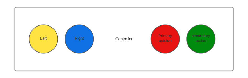
The playable character has 4 actions that it can perform:
- movement on the x-axis (left / right)
- jump
- ability / use
To perform these action there will be 4 buttons for the user to use.
A joystick is not needed for the movement because the movement is not complex, so button fulfill this.
The layout will be as follows:
## Input handling:
The hardware consist out of a microcontroller and a FPGA.
The microcontroller will process the game logic.
For this reason the input will be handled by the microcontroller as this will improve playability (stated in research).
The controller will have four buttons, so 4 data pins are needed on the microcontroller plus a ground and 3.3V or 5V pin.
In total there are 6 pins needed.
If the game is going to be played by 2 person, there are 4 more data pins needed so 8 data pins for both controllers.
For data transfer between STM32 and FPHA there are 4 pins needed at maximum (SPI for instance).
The STM32 will be used and most STM32 boards have enough I/O pins for our needs.
The STM32 F030 and F091 provided by AVANS both have 15 digital pins and 6 analog pins.
The buttons will be connected as follows:
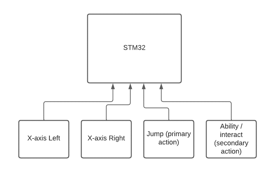
To implement the input in the game, the input should be ckecked at the start of each game cycle. In this case there are no interupts needed.
# STM32 software
# PPU
Here's a list of features our PPU has:
- 320x240 @ 60Hz VGA output (upscaled to 640x480)
- single tilemap with room for 1024 tiles of 16x16 pixels
- 8 colors per palette, with 4096 possible colors (12-bit color depth)
- 640x480 background canvas with scrolling
- NO background scrolling splits
- 128 total sprites on screen (NO scanline sprite limit)
- sprites are always drawn on top of the background layer
- PPU control using DMA (dual-port asynchronous RAM)
- tiles can be flipped using FAM or BAM
- no frame buffer
- vertical and horizontal sync and blank output
Notable differences:
- NES nametable equivalent is called BAM (background attribute register)
- NES OAM equivalent is called FAM (foreground attribute register)
- 320x240 @ 60Hz output
Since we're using VGA, we can't use custom resolutions without an
upscaler/downscaler. This resolution was chosen because it's exactly half of
the lowest standard VGA resolution 640x480.
- No scanline sprite limit
Unless not imposing any sprite limit makes the hardware implementation
impossible, or much more difficult, this is a restriction that will likely
lead to frustrating debugging sessions, so will not be replicated in our
custom PPU.
- Sprites are 16x16
Most NES games already tile multiple 8x8 tiles together into "metatiles" to
create the illusion of larger sprites. This was likely done to save on memory
costs as RAM was expensive in the '80s, but since we're running on an FPGA
cost is irrelevant.
- Single 1024 sprite tilemap shared between foreground and background sprites
The NES OAM registers contain a bit to select which tilemap to use (of two),
which effectively expands each tile's index address by one byte. Instead of
creating the illusion of two separate memory areas for tiles, having one
large tilemap seems like a more sensible solution to indexed tiles.
- 8 total palettes, with 8 colors each
More colors is better. Increasing the total palette count is a very memory
intensive operation, while increaing the palette color count is likely slower
when looking up color values for each pixel on real hardware.
- Sprites can be positioned paritally off-screen on all screen edges using only
the offset bits in the FAM register
The NES has a separate PPUMASK register to control special color effects, and
to shift sprites off the left and top screen edges, as the sprite offsets
count from 0. Our PPU's FAM sprite offset bits count from -15, so the sprite
can shift past the top and left screen edges, as well as the standard bottom
and right edges.
- No status line register, only V-sync and H-sync outputs are supplied back to
CPU
The NES status line register contains some handy lines, such as a buggy
status line for reaching the max sprite count per scanline, and a status line
for detecting collisions between background and foreground sprites. Our PPU
doesn't have a scanline limit, and all hitbox detection is done in software.
Software hacks involving swapping tiles during a screen draw cycle can still
be achieved by counting the V-sync and H-sync pulses using interrupts.
- No background scrolling splits
This feature allows only part of the background canvas to be scrolled, while
another portion stays still. This was used to draw HUD elements on the
background layer for displaying things like health bars or score counters.
Since we are working with a higher foreground sprite limit, we'll use regular
foreground sprites to display HUD elements.
- Sprites are always drawn on top of the background layer
Our game doesn't need this capability for any visual effects. Leaving this
feature out will lead to a simpler hardware design
## Hardware design schematics
### Top (level 1)

Important notes:
- The STM32 can reset the PPU. This line will also be connected to a physical
button on the FPGA.
- The STM32 uses direct memory access to control the PPU.
- The PPU's native resolution is 320x240. It works in this resolution as if it
is a valid VGA signal. The STM32 is also only aware of this resolution. This
resolution is referred to as "tiny" resolution. Because VGA-compatible LCD's
likely don't support this resolution due to low clock speed, a built-in
pixel-perfect 2X upscaler is chained after the PPU's "tiny" output. This
means that the display sees the resolution as 640x480, but the PPU and STM32
only work in 320x240.
- The STM32 receives the TVSYNC and THSYNC lines from the PPU. These are the
VSYNC and HSYNC lines from the tiny VGA signal generator. These lines can be
used to trigger interrupts for counting frames, and to make sure no
read/write conflicts occur for protected memory regions in the PPU.
- NVSYNC, NHSYNC and the RGB signals refer to the output of the native VGA
signal generator.
### Level 2

Important notes:
- The pixel fetch logic is pipelined in 5 stages:
1. - (Foreground sprite info) calculate if foreground sprite exists at
current pixel using FAM register
- (Background sprite info) get background sprite info from BAM register
2. - (Sprite render) calculate pixel to read from TMM based on sprite info
3. - (Compositor) get pixel with 'highest' priority (pick first foreground
sprite with non-transparent color at current pixel in order, fallback to
background)
- (Palette lookup) lookup palette color using palette register
- (VGA signal generator) output real color to VGA signal generator
- The pipeline stages with two clock cycles contain an address set and memory
read step.
- The pipeline takes 5 clock ticks in total. About 18 are available during each
pixel. For optimal display compatibility, the output color signal should be
stable before 50% of the pixel clock pulse width (9 clock ticks).
- Since the "sprite info" and "sprite render" steps are fundamentally different
for the foreground and background layer, these components will be combined
into one for each layer respectively. They are separated in the above diagram
for pipeline stage illustration.
- The BAX, FAM, and PAL registers are implemented in the component that
directly accesses them, but are exposed to the PPU RAM bus for writing.
- Each foreground sprite render component holds its own sprite data copy from
the RAM in it's own cache memory. The cache updates are fetched during the
VBLANK time between each frame.
### Level 3
This diagram has several flaws, but a significant amount of time has already
been spent on these, so they are highlighted here instead of being fixed.

Flaws:
- Pipeline stages 1-4 aren't properly connected in this diagram, see level 2
notes for proper functionality
- The global RESET input resets all PPU RAM, but isn't connected to all RAM
ports
- All DATA inputs on the same line as an ADDR output are connections to a
memory component. Not all of these are connected in the diagram, though they
should be.
- All ADDR and ADDR drivers are also tri-state. EN inputs need to be added to
support switching the output on/off.
Important notes:
- The background sprite and foreground sprite component internally share some
components for coordinate transformations
- The foreground sprite component is only shown once here, but is cloned for
each foreground sprite the PPU allows.
- The CIDX lines between the sprite and compositor components is shared by all
sprite components, and is such tri-state. A single sprite component outputs a
CIDX signal based on the EN signal from the compositor.
- All DATA and ADDR lines are shared between all RAM ports. WEN inputs are
controlled by the address decoder.
<!--
## Registers
|Address|Size (bytes)|Alias|Description|
|-|-|-|-|
|`0x00000`|`0x00000`|TMM |[tilemap memory][TMM]|
|`0x00000`|`0x00000`|BAM |[background attribute memory][BAM]|
|`0x00000`|`0x00000`|FAM |[foreground attribute memory][FAM]|
|`0x00000`|`0x00000`|PAL |[palettes][PAL]|
|`0x00000`|`0x00000`|BAX |[background auxiliary memory][BAX]|
[TMM]: #tilemap-memory
### Tilemap memory
- TODO: list format
[BAM]: #background-attribute-memory
### Background attribute memory
- TODO: list format
[FAM]: #foreground-attribute-memory
### Foreground attribute memory
- TODO: list format
[PAL]: #palettes
### Palettes
- TODO: list format
[BAX]: #background-auxiliary-memory
### Background auxiliary memory
- background scrolling
-->
[nesppuspecs]: https://www.copetti.org/writings/consoles/nes/
[nesppudocs]: https://www.nesdev.org/wiki/PPU_programmer_reference
[nesppupinout]: https://www.nesdev.org/wiki/PPU_pinout
[custompputimings]: https://docs.google.com/spreadsheets/d/1MU6K4c4PtMR_JXIpc3I0ZJdLZNnoFO7G2P3olCz6LSc
# APU
|